Explore Module
| Sito: | Bios4You |
| Corso: | (31) The Photovoltaic Journey: Capturing the Sun |
| Libro: | Explore Module |
| Stampato da: | Svečio paskyra |
| Data: | martedì, 25 agosto 2026, 05:56 |
Engagement phase
Guiding question. Can we extract electricity from sunlight without moving parts?
The lesson opens with a brief demonstration: a small solar panel connected to an LED or a calculator. When exposed to light, the device works; when covered, it stops. The purpose is not simply to show that "solar panels work," but to introduce the idea that light energy can be directly converted into electrical energy through solid-state physics-no turbines, no combustion, no mechanical motion required.
Initial stimuli (videos and short resources)
How do solar panels work? TED-Ed: a clear animated overview of photovoltaic cells, the P-N junction, and electron flow.
Solar Energy Basics – U.S. Department of Energy: an accessible introduction to photovoltaic technology and renewable energy systems.
https://www.energy.gov/eere/solar/solar-photovoltaic-technology-basics
Photoelectric Effect: photoelectric Effect: interactive exploration of how photons interact with metal surfaces to eject electrons, demonstrating quantum properties of light.
https://phet.colorado.edu/en/simulations/photoelectric
A quick demonstration or video clip showing a solar cell powering a small motor or charging a battery invites students to ask, "How does light become electricity without wires moving or chemicals reacting?"
The goal is to highlight that energy conversion is a quantum process occurring at the atomic level within semiconductor materials, not a macroscopic mechanical or thermal transformation.
Suggested video: How Solar Panels Work (SciShow)
Brainstorming activities in the classroom
Leading question. Without light, there is no photovoltaic current: what happens to photons as they enter the solar cell, and how do they generate an electrical signal that can power devices?
Prompting questions
The photon's energy must exceed the semiconductor's bandgap; silicon's bandgap (~1.1 eV) means only photons with wavelengths shorter than ~1100 nm (visible and near-infrared light) can free electrons and generate current.
Because photons with energy below the bandgap pass through without generating charge carriers, while photons with much higher energy waste excess energy as heat. This is why single-junction silicon cells have a theoretical maximum efficiency of ~33% (Shockley-Queisser limit).
Does the solar cell "store" electricity like a battery?
No; the solar cell generates current only when illuminated. The photovoltaic effect produces charge separation and flow in real-time; to store energy, an external battery or capacitor is needed.
Because light intensity (photon flux) directly affects the number of electron-hole pairs generated. Lower intensity means fewer photons, fewer charge carriers, and reduced current output. Voltage remains relatively stable, but current drops significantly.
Label the layers of a solar cell (anti-reflective coating, N-type silicon, P-N junction, P-type silicon, back contact) using a worksheet or an interactive diagram.
Suggested resource: Solar Cell Structure Diagram - Encyclopædia Britannica
https://www.britannica.com/technology/solar-cell
Physics of Solar Energy Conversion
Light, absorption, and photon energy
Solar energy conversion begins when photons from sunlight strike the surface of a photovoltaic cell. Sunlight is a mixture of electromagnetic waves spanning ultraviolet, visible, and infrared wavelengths. Each photon carries a discrete packet of energy determined by its wavelength: shorter wavelengths (blue light) carry more energy than longer wavelengths (red light).
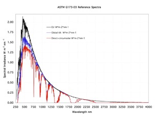
Figure 2. Solar spectral irradiance (ASTM G173-03 reference spectra) showing the distribution of photon energy across wavelengths. Silicon solar cells with a bandgap of ~1.1 eV (corresponding to ~1100 nm wavelength) can only convert visible and near-infrared photons. (Source: NREL)
When a photon enters a semiconductor material like silicon, it may be absorbed, reflected, or transmitted.
Absorption is key: if the photon's energy equals or exceeds the material's bandgap energy (the minimum energy required to free an electron from its atomic bond), the electron is promoted from the valence band to the conduction band.
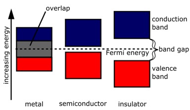
Figure 3. Comparison of energy band structures in metals, semiconductors, and insulators. In semiconductors like silicon, the band gap (Eg ≈ 1.1 eV) is small enough that photons can excite electrons from the valence band (red) to the conduction band (blue), enabling photovoltaic energy conversion. (Source: Wikimedia Commons, Public Domain)
This creates an electron-hole pair-a mobile negative charge (electron) and a corresponding positive vacancy (hole).
What determines whether a photon is absorbed or passes through?
The relationship between photon energy and the semiconductor's bandgap. Silicon's bandgap is ~1.1 eV, corresponding to infrared light at ~1100 nm. Photons with less energy pass through; photons with much more energy generate heat after freeing electrons.
From photons to electrons: the P-N junction
The absorbed photon creates an electron-hole pair, but without an internal electric field, these charges would quickly recombine, releasing energy as heat rather than electricity. This is where the P-N junction becomes essential.
Silicon is "doped" with impurities to create two distinct regions:
- N-type silicon: doped with phosphorus (extra electrons → negative charge carriers)
- P-type silicon: doped with boron (deficit of electrons → positive "holes")
At the boundary between N-type and P-type regions, a depletion zone forms naturally. Electrons from the N-side diffuse across to fill holes on the P-side, leaving behind positively charged atoms on the N-side and negatively charged atoms on the P-side. This charge separation creates a built-in electric field pointing from N to P.
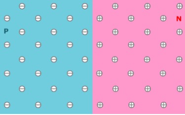
Figure 4. Schematic representation of a P-N junction before equilibrium. The P-type region (left, cyan) contains excess holes (positive charge carriers), while the N-type region (right, pink) contains excess electrons (negative charge carriers). When the two regions are brought into contact, charge carriers diffuse across the junction. (Source: PVEducation.org, educational use)
When a photon generates an electron-hole pair near the junction, the electric field sweeps the electron toward the N-side and the hole toward the P-side. This separation prevents recombination and drives charge carriers in opposite directions, creating a voltage difference between the two sides of the cell.
Because the electric field at the P-N junction provides a driving force stronger than random thermal motion, directing electrons and holes away from each other before they can recombine.
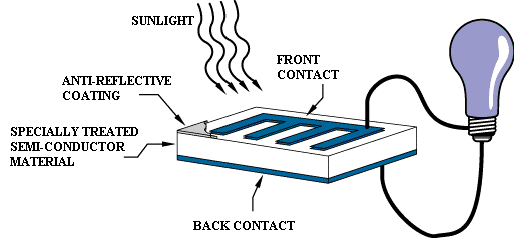
Figure 5. Complete solar cell operation showing the conversion of sunlight into electrical current. Photons strike the semiconductor material through the anti-reflective coating, generating electron-hole pairs that are separated by the internal electric field. The electrons flow through the external circuit (represented by the light bulb) before returning to recombine, creating usable electrical power. (Source: Wikimedia Commons, Public Domain)
Layered structure and charge collection
A typical silicon solar cell has multiple layers optimized for light absorption and charge collection:
- Anti-reflective coating (top): reduces reflection, maximizing photon entry
- N-type silicon (thin layer): electron-rich region where electrons are collected
- P-N junction (interface): where the electric field separates charge carriers
- P-type silicon (thicker base): where holes are collected
- Metal contacts (top and bottom): conduct electrons out to an external circuit
The front contact is designed as a grid pattern to minimize shading while collecting current. The back contact covers the entire rear surface for maximum conductivity.
Why is the N-layer thinner than the P-layer?
Because most photons are absorbed near the surface; a thin N-layer ensures photo-generated carriers are close to the junction's electric field for efficient separation, while the thicker P-layer absorbs longer-wavelength photons deeper in the material.
From the junction to the circuit: current and voltage
When sunlight illuminates the cell, continuous photon absorption generates a steady supply of electron-hole pairs. The junction's electric field continuously separates these charges, driving electrons toward the N-side and holes toward the P-side.
When metal contacts are attached and connected through an external circuit, electrons flow from the N-side, through the circuit (powering a load), and return to the P-side to recombine with holes. This flow constitutes photovoltaic current.
The voltage produced by a single silicon cell is approximately 0.5–0.6 volts, determined by the bandgap energy and junction characteristics. Current depends on light intensity and cell area: more photons → more electron-hole pairs → higher current.
Multiple cells are connected in series (positive terminal of one to negative terminal of the next) to add voltages. A typical panel contains 60–72 cells in series, producing 30–40 volts under standard conditions.
From theory to everyday objects
The same principles operating in solar cells are found in:
- Solar calculators: small cells providing milliwatts of power for low-energy devices
- Rooftop solar panels: arrays of series-connected cells generating kilowatts for homes
- Solar farms: large-scale installations producing megawatts for the electrical grid
- Space satellites: high-efficiency multi-junction cells powering spacecraft where reliability is critical
Bringing quantum physics out of the abstract helps students understand not only how photovoltaics work, but why design choices (bandgap selection, anti-reflective coatings, cell thickness) directly impact real-world energy performance.
Let’s reflect together.
Converting sunlight into electricity requires precise control at the atomic level. If the P-N junction is essential for charge separation, why can't we use any semiconductor? What role does doping play in creating the internal electric field? How do temperature, shading, and material quality affect the efficiency of energy conversion?
Web-based resources
How do solar panels work? – TED-Ed
https://www.youtube.com/watch?v=xKxrkht7CpY
Animated explanation of photovoltaic cells and electron flow.
Solar Photovoltaic Technology Basics – U.S. Department of Energy
https://www.energy.gov/eere/solar/solar-photovoltaic-technology-basics
Overview of PV technology and solar energy conversion.
PhET – Photoelectric Effect
https://phet.colorado.edu/en/simulations/photoelectric
Interactive exploration of photon energy and electron ejection.
Advanced Level
Quantum mechanics of photovoltaic conversion
The photovoltaic effect is fundamentally a quantum phenomenon. When a photon is absorbed by a silicon atom, its energy must overcome the bandgap energy (Eg ≈ 1.1 eV for crystalline silicon) to promote an electron from the valence band to the conduction band. This process creates an electron-hole pair with a probability determined by the material's absorption coefficient and photon energy.
Energy losses occur at multiple stages:
- Photons with E < Eg pass through without generating charge carriers (transmission losses)
- Photons with E >> Eg generate "hot" carriers that quickly lose excess energy as heat through thermalization
- Surface reflection (without anti-reflective coating, ~30% of incident light is lost)
- Recombination (electron-hole pairs recombine before reaching contacts, releasing energy as heat or light)
The Shockley-Queisser limit establishes the theoretical maximum efficiency for a single-junction solar cell at ~33% under standard solar spectrum (AM1.5G). Real-world silicon cells achieve 15–22% due to additional losses from resistance, imperfect materials, and non-ideal junction properties.
Efficiency, spectral response, and material optimization
Solar cell efficiency depends critically on how well the semiconductor's bandgap matches the solar spectrum. Silicon's 1.1 eV bandgap is a compromise: it captures visible and near-infrared light effectively but cannot utilize lower-energy infrared photons or fully exploit high-energy ultraviolet photons.
Advanced strategies to overcome the Shockley-Queisser limit:
- Multi-junction (tandem) cells: Stack semiconductors with different bandgaps (e.g., GaInP/GaAs/Ge) so each layer absorbs a specific portion of the spectrum. Lab efficiencies exceed 47% under concentrated sunlight.
- Perovskite cells: Hybrid organic-inorganic materials with tunable bandgaps, rapid charge transport, and solution-processable fabrication. Current efficiencies approach 26%, but stability and scalability remain challenges.
- Hot carrier cells (experimental): Harvest energy from hot carriers before thermalization, potentially exceeding 66% efficiency. Requires ultrafast charge extraction mechanisms not yet commercially viable.
Why do high-energy photons reduce overall efficiency?
Because excess energy above the bandgap is rapidly lost as heat through phonon emission (thermalization) within picoseconds. A 3 eV photon (UV) generates the same single electron-hole pair as a 1.2 eV photon (red), wasting 1.9 eV as heat.
Why can't we simply use a very small bandgap to capture all photons?
Because smaller bandgaps produce lower voltage (V ∝ Eg), and thermal generation of carriers increases, raising "dark current" that reduces net efficiency. There's an optimal bandgap (~1.1–1.4 eV) balancing photon absorption and voltage output.
Charge transport, recombination, and device physics
After generation at the junction, charge carriers must travel to the contacts without recombining. Recombination mechanisms limit efficiency:
- Radiative recombination: electron-hole pairs recombine, emitting photons (significant in direct-bandgap materials like GaAs, minimal in silicon)
- Auger recombination: three-particle interaction where energy is transferred to a third carrier instead of emitted as light (increases at high carrier densities)
- Shockley-Read-Hall (SRH) recombination: defects and impurities in the crystal lattice trap carriers, facilitating recombination (dominates in lower-quality silicon)
High-quality crystalline silicon minimizes SRH recombination through controlled manufacturing. Passivation layers (e.g., silicon nitride, aluminum oxide) on surfaces reduce interface recombination. Doping profiles are optimized so the electric field extends across the active region, ensuring rapid carrier separation.
Why does temperature reduce solar cell efficiency?
Because higher temperature increases lattice vibrations (phonons), which scatter charge carriers, reduce mobility, and increase recombination rates. Additionally, the bandgap decreases slightly with temperature (~–0.3 meV/K for silicon), reducing voltage output. Typical efficiency loss: ~0.4% per °C above 25°C.
System integration and real-world performance
A photovoltaic system includes not just solar cells, but:
- Inverters: convert DC output to AC for grid compatibility
- Maximum Power Point Tracking (MPPT): continuously adjusts load to extract maximum power as light conditions change
- Energy storage (optional): batteries store excess generation for nighttime or cloudy periods
- Grid connection: feed surplus energy to the electrical grid, often with net metering policies
Capacity factor (actual energy output / theoretical maximum) for solar installations is typically 15–25%, constrained by:
- Day/night cycles
- Weather variability
- Seasonal changes in sun angle
- System losses (wiring resistance, inverter inefficiency, shading)
Why do solar panels degrade over time?
UV exposure, moisture ingress, thermal cycling, and potential-induced degradation (PID) gradually reduce efficiency. High-quality modules lose ~0.5% efficiency per year; warranties typically guarantee 80% output after 25 years.
Let's reflect together
Why do modern solar cells still operate far below the Shockley-Queisser limit?
Because real-world materials have defects, surfaces introduce recombination, and charge extraction isn't perfectly efficient. Bridging the gap between theoretical and practical performance drives ongoing research in material science and device engineering.
Why can't we achieve 100% efficiency even with perfect materials?
Because fundamental thermodynamic and quantum mechanical constraints apply: not all photons can be absorbed (spectral mismatch), thermalization wastes high-energy photons, and maintaining voltage output requires some energy dissipation. The second law of thermodynamics ultimately limits conversion efficiency.
Flipped Learning
Objective. Prepare for classroom discussion by understanding the sequence photon → absorption → charge separation → current flow and the physics/engineering connections in photovoltaic systems.
Tasks (to be submitted as a 1–2-page report or 6–8 slides):
1. Short reading on the structure of a silicon solar cell and the path of photons. Highlight: anti-reflective coating, N-type layer, P-N junction, P-type layer, metal contacts.
- Worksheet "N-type vs. P-type Silicon": complete a table with:
- Doping element (phosphorus/boron)
- Majority charge carrier (electrons/holes)
- Role in charge separation
- Position in cell structure (top/bottom)
- PhET Semiconductors simulation: create two screenshots -
a. Intrinsic (undoped) silicon: observe energy bands and lack of free carriers
b. Doped silicon (N+P junction): observe band bending, built-in electric field, and charge separation under illumination - Short synthesis (max 120 words): explain in your own words how the solar cell does not "collect" sunlight like a thermal panel but converts photon energy into separated electrical charges through quantum absorption and junction physics.
- Three debriefing questions:
- One on quantum physics: Why must photon energy exceed the bandgap?
- One on materials science: How does doping create an electric field?
- One on systems engineering: Why do solar panels produce DC but homes use AC?
Submission. Upload the PDF or slides to the class channel before the lesson.